-
CN
-
Service Hotline
+8618129931046 Mr. Liao


Time:2026-01-08 Views:1

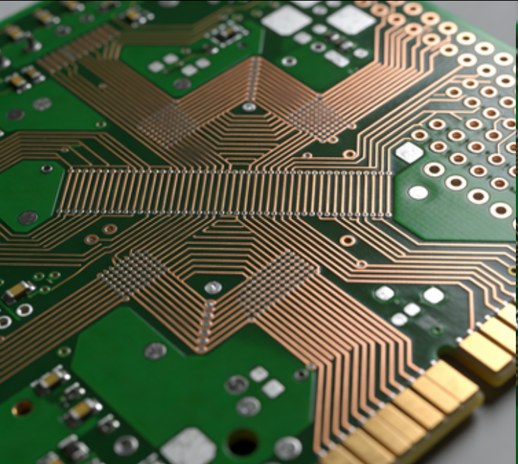
Printed Circuit Boards suitable for Radio Frequency (RF) circuits are specialized and meticulously designed to meet the stringent requirements of high - frequency signal transmission and processing. RF circuits operate at frequencies ranging from a few megahertz to several gigahertz, where even the slightest design flaws can lead to significant signal degradation, interference, and performance loss. Therefore, the design and manufacturing of RF - suitable PCBs demand a deep understanding of RF principles, precise material selection, and advanced fabrication techniques.
One of the primary considerations in designing RF - suitable PCBs is the selection of appropriate substrate materials. The substrate material's dielectric constant (Dk) and dissipation factor (Df) play crucial roles in determining the characteristic impedance and signal loss of the RF traces. Low - loss materials with stable dielectric properties, such as Rogers RT/duroid, Taconic TLY, and Isola FR408HR, are commonly used. These materials minimize signal attenuation and phase distortion over high frequencies, ensuring that the RF signals can travel along the traces with minimal degradation. Additionally, the thickness and uniformity of the substrate are carefully controlled to maintain consistent impedance throughout the PCB.
The layout design of RF - suitable PCBs is another critical aspect. RF traces need to be routed with extreme precision to avoid unwanted signal reflections, crosstalk, and radiation. Short and straight traces are preferred to minimize signal path lengths and reduce the effects of parasitic capacitance and inductance. Differential signaling is often employed for RF signals to improve immunity to electromagnetic interference (EMI) and common - mode noise. Ground planes are also strategically placed to provide a return path for the RF signals and shield them from external interference. Moreover, proper isolation between different RF components and circuits is essential to prevent interference between them, which may involve using shielding enclosures or isolation slots in the PCB layout.
Manufacturing RF - suitable PCBs requires advanced techniques to ensure high - quality and reliable performance. Precise etching processes are used to create fine - pitch RF traces with tight tolerances. Surface finishing options, such as immersion gold or electroless nickel immersion gold (ENIG), are selected to provide good electrical conductivity and corrosion resistance for the RF pads and traces. Additionally, controlled impedance manufacturing processes are employed to ensure that the characteristic impedance of the RF traces matches the requirements of the RF circuits. With their carefully engineered design and manufacturing, PCBs suitable for RF circuits are essential for enabling the reliable operation of various RF - based devices, including wireless communication equipment, radar systems, and satellite receivers.