-
CN
-
Service Hotline
+8618129931046 Mr. Liao


Time:2025-04-18 Views:1

Component Placement and Soldering in SMT
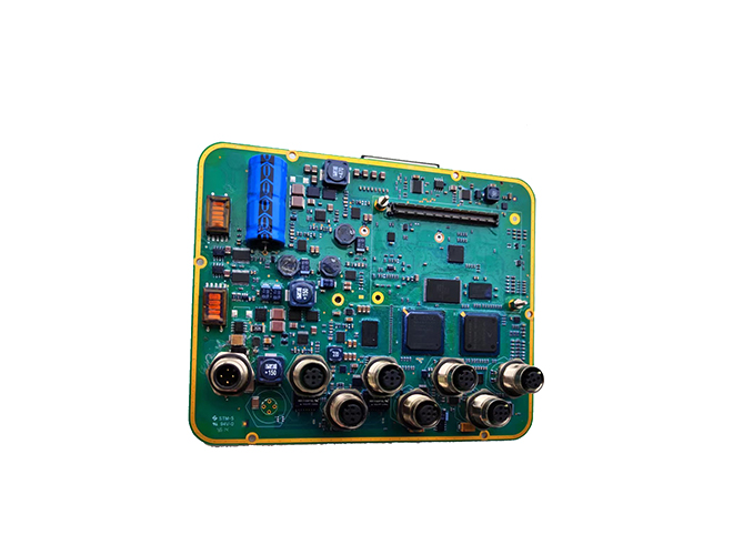
SMT allows for the placement of components directly on the surface of the printed circuit board without the need for through - hole drilling as in traditional through - hole technology. The process starts with the application of solder paste to the pads on the PCB. This is typically done using a stencil printer, where a metal stencil with precisely cut openings corresponding to the PCB pad layout is placed over the board, and solder paste is squeegeed through the openings onto the pads. Then, surface - mount components, which are much smaller in size compared to through - hole components, are picked up by a pick - and - place machine using vacuum - tipped nozzles. The machine precisely places the components on the solder - pasted pads according to the programmed coordinates. Once the components are placed, the PCB is subjected to reflow soldering. The reflow process, as described earlier, melts the solder paste, creating strong electrical and mechanical connections between the components and the PCB. This method of component placement and soldering enables higher component density on the PCB, as surface - mount components can be placed closer together compared to through - hole components.
Advantages of SMT in PCBA
One of the major advantages of SMT in PCBA is its ability to reduce the size and weight of the final product. The smaller size of surface - mount components and the elimination of through - hole drilling allow for more compact PCB designs. This is especially crucial in modern electronic devices such as smartphones, tablets, and wearable electronics, where space is at a premium. SMT also offers higher assembly efficiency. The automated pick - and - place machines can place a large number of components in a short time, significantly increasing the production throughput. Moreover, SMT provides better electrical performance. The shorter lead lengths of surface - mount components result in reduced parasitic capacitance and inductance, which is beneficial for high - frequency applications. For example, in high - speed data transmission circuits, SMT components can help in maintaining signal integrity. In addition, SMT is more cost - effective in the long run. Although the initial investment in SMT equipment such as pick - and - place machines and reflow ovens is high, the reduced component costs (due to smaller size and higher integration), lower labor costs (because of automation), and higher production yields make it a cost - efficient choice for large - scale PCBA production.
Challenges and Solutions in SMT Application
However, the application of SMT in PCBA also comes with some challenges. One of the main challenges is the handling of small - sized components. As components continue to shrink in size, it becomes more difficult to accurately place them on the PCB. Advanced pick - and - place machines with high - precision vision systems are used to address this issue. These machines can detect the exact position of the component and the PCB pads, ensuring accurate placement. Another challenge is the soldering of fine - pitch components. Components with very small lead pitches are more prone to solder bridges and other soldering defects. To overcome this, special solder pastes with finer particle sizes are used, and the reflow temperature profile is carefully optimized. In addition, advanced inspection techniques such as high - magnification AOI and X - ray inspection are essential to detect and correct any soldering defects in fine - pitch SMT components. Despite these challenges, the benefits of SMT in PCBA far outweigh the drawbacks, making it the dominant technology in modern electronic manufacturing.