-
CN
-
Service Hotline
+8618129931046 Mr. Liao


Time:2025-06-05 Views:1

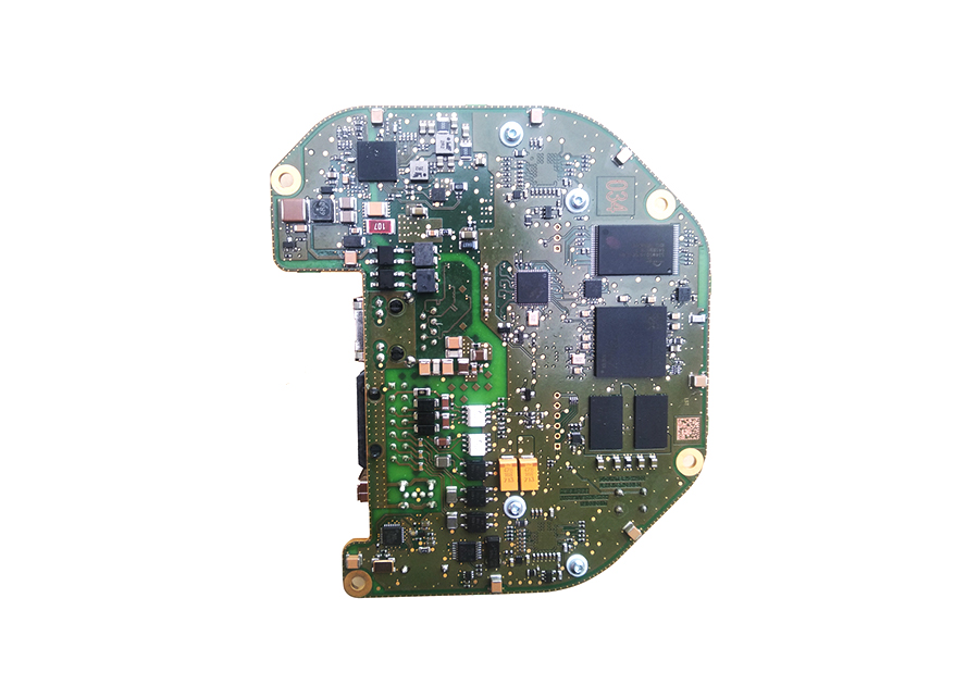
Vias are an essential part of multilayer printed circuit boards (PCBs), providing electrical connections between different layers. Understanding the current - carrying capacity of vias is crucial for ensuring the reliable operation of PCBs, especially in high - power applications.
Factors Affecting Vias' Current - Carrying Capacity
The diameter of the via is a primary factor influencing its current - carrying capacity. Larger - diameter vias can generally carry more current. This is because a larger cross - sectional area allows for more electrons to flow through without overheating. For example, a via with a diameter of 0.5 mm can carry a significantly higher current compared to a via with a diameter of 0.1 mm. However, increasing the via diameter may also take up more space on the PCB, which can be a limitation in high - density designs.
The material of the via also plays a vital role. Copper is the most commonly used material for vias in PCBs due to its excellent electrical conductivity. The thickness of the copper plating on the via wall affects its current - carrying capacity. A thicker copper plating provides a lower resistance path for the current, enabling the via to carry more current. Additionally, the number of vias in parallel can increase the overall current - carrying capacity. In high - power applications, multiple vias are often used in parallel to distribute the current and prevent any single via from overheating. For instance, in a power - supply layer of a PCB for a high - performance graphics card, dozens of vias may be used in parallel to carry the large amount of current required by the graphics processing unit.
Calculating Vias' Current - Carrying Capacity
There are several methods for calculating the current - carrying capacity of vias. One commonly used formula is based on the circular mil - ampere rule. According to this rule, the current - carrying capacity (I) of a circular conductor (such as a via) can be estimated as I = k * A, where A is the cross - sectional area of the conductor in circular mils and k is a constant that depends on factors such as the type of material, the temperature rise allowed, and the cooling conditions. For copper vias in a typical PCB environment, with a maximum allowable temperature rise of 10°C, k is approximately 10. Another approach is to use empirical data and look - up tables provided by PCB manufacturers or industry standards organizations. These tables take into account various factors such as via diameter, copper thickness, and the number of vias in parallel to provide approximate current - carrying capacity values.
Design Considerations for Vias in High - Current Applications
In high - current applications, proper design of vias is essential. As mentioned earlier, using multiple vias in parallel is a common strategy. The vias should be evenly distributed to ensure uniform current distribution. Additionally, the connection pads of the vias should be large enough to handle the current without excessive heating. Thermal vias can also be incorporated around the high - current - carrying vias to help dissipate heat. These thermal vias are connected to a heat - sinking layer or an external heat sink. For example, in a PCB for an industrial power inverter, thermal vias may be used to transfer heat from the high - current - carrying vias in the power - switching section to a metal core layer, which acts as a heat sink. Moreover, when designing vias for high - current applications, it's important to consider the overall layout of the PCB to minimize the resistance and inductance in the current path, which can affect the performance of the circuit.