-
CN
-
Service Hotline
+8618129931046 Mr. Liao


Time:2025-05-13 Views:1

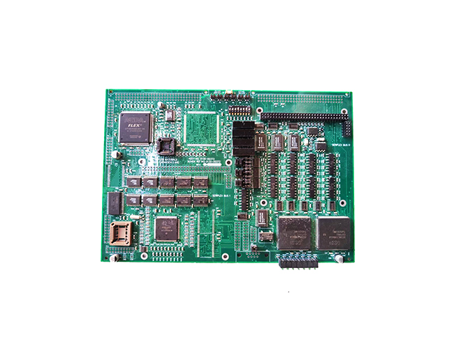
The design and manufacturing of multilayer printed circuit boards (PCBs) represent a sophisticated and highly specialized area within the electronics industry. Multilayer PCBs are composed of multiple layers of conductive traces, separated by insulating materials, and interconnected through vias. This design allows for a higher component density, more complex circuit routing, and improved electrical performance compared to single - or double - layer PCBs.
The design process of multilayer PCBs begins with a detailed understanding of the electrical requirements of the circuit. Engineers need to carefully plan the placement of components, power and ground planes, and signal traces to ensure optimal performance. Power and ground planes are typically included in multilayer PCBs to provide a stable power supply and reduce electromagnetic interference. These planes are large, continuous layers of copper that distribute power and ground signals evenly across the board. Signal traces are then routed on the remaining layers, with careful consideration given to factors such as signal integrity, crosstalk, and impedance matching.
In high - speed applications, such as in telecommunications and computer systems, the design of multilayer PCBs becomes even more critical. High - speed signals are sensitive to factors like trace length, trace width, and the presence of vias. To maintain signal integrity, designers use techniques such as controlled - impedance routing, where the impedance of the signal traces is carefully controlled to match the impedance of the connected components. Additionally, measures are taken to minimize crosstalk between adjacent signal traces, such as using proper trace spacing and shielding.
The manufacturing process of multilayer PCBs is complex and involves multiple steps. It starts with the preparation of individual copper - clad laminates, which are then drilled to create holes for vias. The vias are used to connect the different layers of the PCB, allowing electrical signals to pass through. After drilling, the vias are plated with copper to create a conductive pathway. Next, the layers are aligned and bonded together using a combination of heat and pressure, with an insulating material, such as prepreg, between the layers. The board is then processed through a series of steps, including imaging, etching, and surface finishing, to create the final PCB.
Quality control is an essential part of the multilayer PCB manufacturing process. Advanced inspection techniques, such as X - ray inspection and automated optical inspection, are used to ensure the integrity of the vias, the accuracy of the trace routing, and the overall quality of the board. Any defects or inconsistencies can significantly impact the performance of the PCB and the electronic system it is part of. With the increasing demand for smaller, more powerful, and more complex electronic devices, the design and manufacturing of multilayer PCBs will continue to play a vital role in enabling technological advancements in various industries.