-
CN
-
Service Hotline
+8618129931046 Mr. Liao


Time:2025-05-08 Views:1

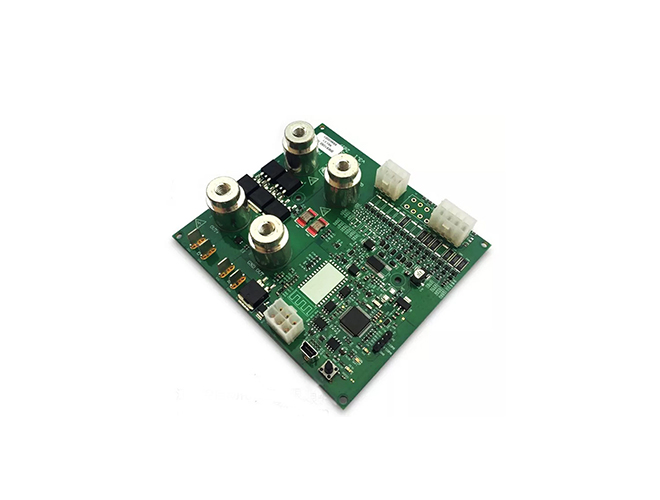
High - precision printed circuit boards (PCBs) are at the heart of advanced electronic systems, demanding the utmost accuracy and attention to detail in their design and manufacturing. These boards are essential for applications where signal integrity, miniaturization, and reliability are of critical importance, such as in aerospace, medical devices, high - performance computing, and telecommunications.
The defining characteristic of high - precision PCBs is their ability to support extremely fine - pitch components and intricate circuit layouts. With the continuous miniaturization of electronic components, high - precision PCBs need to accommodate component footprints with pad pitches as small as 0.2 mm or even less. This requires the use of advanced manufacturing techniques. For instance, laser drilling is often employed instead of traditional mechanical drilling for vias, as lasers can create holes with diameters as small as 0.1 mm with high precision, minimizing the impact on the board's overall size and performance.
In terms of trace widths and spacing, high - precision PCBs can achieve line widths and spaces as narrow as 0.075 mm or less. To ensure such fine features, photolithography processes with high - resolution masks are used. The masks are created using electron - beam or laser - writing technologies, which can produce patterns with sub - micron accuracy. This level of precision is crucial for maintaining signal integrity, especially in high - frequency applications. At high frequencies, even the slightest deviation in trace length, width, or impedance can lead to signal attenuation, reflection, and crosstalk.
Another aspect of high - precision PCB manufacturing is the control of board thickness and flatness. Tight tolerances are maintained for the thickness of each layer, as well as the overall board thickness, to ensure proper component mounting and compatibility with other system components. Advanced lamination processes, combined with precise control of temperature, pressure, and time, are used to achieve consistent thickness and flatness across the board. Quality control in high - precision PCB production is rigorous, involving multiple inspection steps. In addition to AOI, X - ray inspection is often used to check the internal structure of the board, including the alignment of vias and the integrity of buried and blind vias. High - precision PCBs not only enable the development of cutting - edge electronic products but also set the standard for quality and performance in the PCB manufacturing industry.