-
CN
-
Service Hotline
+8618129931046 Mr. Liao


Time:2025-11-27 Views:1

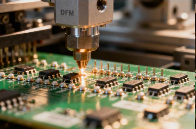
Manufacturability-Oriented PCBA Design (also known as Design for Manufacturability, DFM) is a design approach that optimizes printed circuit board assemblies to align with mass production processes, minimizing manufacturing defects, reducing assembly time, and ensuring consistency across large production runs. Unlike design focused solely on functionality, DFM prioritizes compatibility with automated assembly equipment (e.g., pick-and-place machines, reflow ovens) and standard manufacturing practices—critical for lowering production costs and accelerating time-to-market in industries like consumer electronics, automotive, and IoT.
The core of DFM lies in adhering to manufacturing constraints and simplifying assembly steps. Key technical considerations include: 1) Component Selection for Manufacturability: Choosing components with standard, widely available footprints (e.g., 0402, 0603 for passives) instead of custom or obsolete packages, which are harder to source and handle. Surface-mount technology (SMT) components are preferred over through-hole (THT) where possible, as SMT is faster to assemble and compatible with automated pick-and-place. For THT components (e.g., connectors), ensuring they have sufficient lead length (3-5mm) for wave soldering and are placed on one side of the board to avoid flipping the PCB during assembly. 2) PCB Layout for Assembly: Maintaining minimum component spacing (e.g., ≥0.1mm between components, ≥0.2mm from component to board edge) to prevent pick-and-place errors and ensure proper solder joint formation. Designing clear, non-overlapping solder masks (with opening size 1.2x the pad size) to protect traces and ensure accurate soldering. Adding fiducial marks (2-3 per board, typically 1mm diameter) on the PCB—these are used by pick-and-place machines to calibrate component placement, reducing alignment errors. 3) Solder Joint Reliability: Ensuring pad sizes match component leads (e.g., pad width 1.1x lead width for resistors) to prevent insufficient or excessive solder, which can cause joint failure. Avoiding “tombstoning” (a defect where passive components stand upright) by balancing pad sizes for 0402 and smaller components and placing them parallel to the direction of reflow oven conveyor movement. 4) Panelization Design: Grouping multiple PCBs into a single panel (panelization) to optimize material usage and speed up assembly. Including breakaway tabs (with V-scores or mousebites) between PCBs for easy separation post-assembly, and ensuring panel edges have tooling holes (3-4mm diameter) for handling by manufacturing equipment.
DFM implementation requires collaboration with manufacturing teams early in the design process. Engineers use DFM analysis tools (e.g., Mentor Graphics DFM Checker, Altium DFM Analyzer) to automatically check the design against 100+ manufacturing rules (e.g., component spacing, pad size, solder mask coverage) and flag issues like insufficient clearance or non-standard footprints. Physical prototyping with a small batch (10-20 units) is critical to validate manufacturability—testing assembly efficiency, identifying defects, and refining the design before mass production.
Application scenarios highlight DFM’s impact. In consumer electronics (e.g., smartphone PCBs), DFM ensures 0201-sized passives are placed accurately by pick-and-place machines, reducing defect rates to <0.1%. In automotive PCBs (e.g., ADAS modules), DFM optimizes solder joint design to withstand vibration and temperature cycles, ensuring long-term reliability. In high-volume IoT devices (e.g., smart bulbs), DFM panelization reduces material waste by 15-20% and cuts assembly time per unit by 30%. With manufacturing defects accounting for up to 40% of product failures, DFM is essential for delivering cost-effective, reliable PCBs at scale.