-
CN
-
Service Hotline
+8618129931046 Mr. Liao


Time:2025-05-08 Views:1

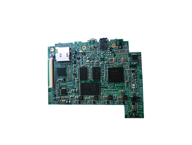
Multilayer printed circuit board (PCB) rapid prototyping has become a crucial process in the electronics industry, enabling the swift realization of complex circuit designs. As electronic devices evolve to be more compact, powerful, and feature - rich, the demand for multilayer PCBs, which stack multiple conductive layers separated by insulating materials, has surged. Rapid prototyping of these boards allows designers and engineers to quickly test and validate their concepts, significantly reducing the time - to - market for new products.
The rapid prototyping process for multilayer PCBs involves several key steps. First, the design files, typically in Gerber format, are generated using specialized PCB design software. These files contain detailed information about the layout of traces, vias, pads, and component footprints on each layer. Subsequently, the data is transferred to advanced manufacturing equipment. High - speed CNC (Computer Numerical Control) drilling machines are employed to create holes for vias, which connect different layers, with extreme precision. The drilling process must be accurate to ensure proper electrical connectivity between layers.
Next, the copper layers are patterned through a process called photolithography. A light - sensitive film is applied to the copper - clad laminates, and the design is transferred onto the film using ultraviolet light. The areas exposed to light become insoluble and are then etched away, leaving behind the desired copper traces. For multilayer PCBs, this process is repeated for each layer, and precise alignment is crucial to ensure that the vias and traces on different layers match up correctly. After patterning, the layers are laminated together using high - pressure and high - temperature processes, with prepreg materials acting as the adhesive between the copper layers and providing electrical insulation.
To expedite the process, many PCB manufacturers have invested in state - of - the - art equipment and optimized their workflows. Some use automated optical inspection (AOI) systems to quickly detect any manufacturing defects, such as short circuits or open circuits, right after the patterning and lamination stages. This enables immediate corrective actions, reducing the time wasted on producing faulty boards. Additionally, advanced software solutions are used to manage the production schedule and prioritize orders, ensuring that multilayer PCB prototypes are delivered within a short turnaround time, often as fast as 24 - 48 hours for simple designs. Rapid prototyping of multilayer PCBs not only accelerates the development cycle but also allows for cost - effective iterations, as any design flaws can be identified and rectified early in the process.