-
CN
-
Service Hotline
+8618129931046 Mr. Liao


Time:2025-04-23 Views:1

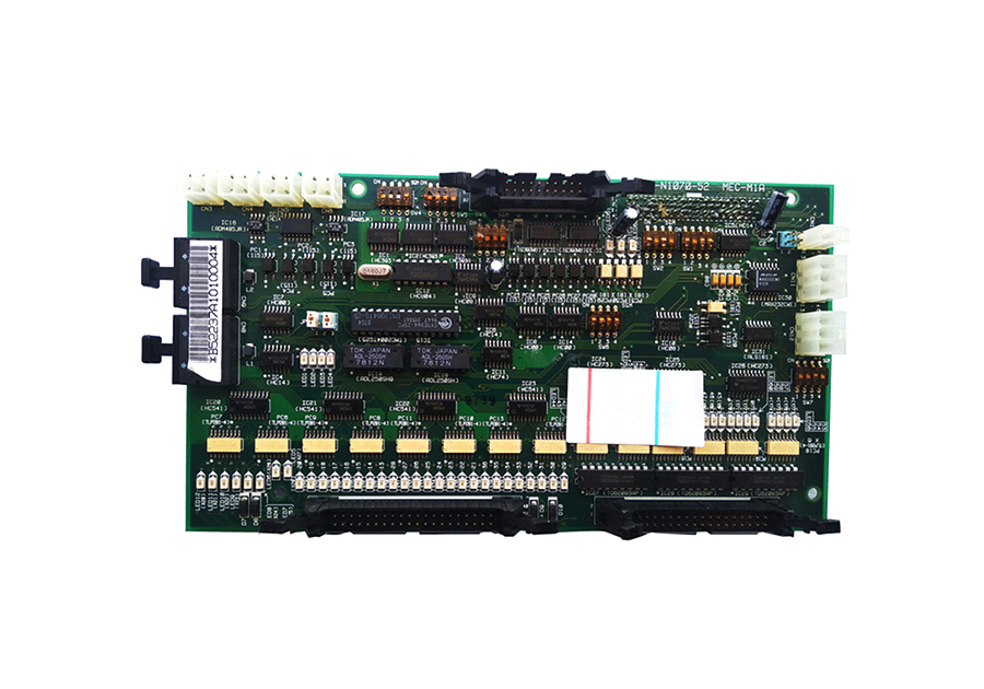
PCBA control board development is a complex and multi-faceted process that involves a series of steps from conceptualization to the final production of a functional printed circuit board assembly used for control purposes. This process requires a combination of electrical engineering, software development, and mechanical design skills to create a control board that meets specific application requirements.
The development process typically starts with requirements gathering. Engineers work closely with end-users or product managers to understand the intended functionality of the control board. This includes defining the input and output interfaces, the control algorithms to be implemented, the operating environment (such as temperature, humidity, and vibration conditions), and any regulatory requirements. For example, in the development of a control board for a smart home appliance, the requirements may include connectivity to a wireless network, control of motor speeds, and integration with a mobile app for remote operation.
Once the requirements are defined, the next step is the schematic design. Electrical engineers use specialized design tools to create a schematic diagram that represents the electrical components and their interconnections on the control board. This involves selecting appropriate components such as microcontrollers, sensors, actuators, and power management ICs based on the requirements. The schematic design also includes considerations for signal integrity, power distribution, and electromagnetic compatibility. After the schematic is completed, it undergoes a thorough review to ensure accuracy and compliance with the design requirements.
Following the schematic design is the printed circuit board (PCB) layout. The PCB layout engineer takes the schematic and arranges the components and traces on the physical board. This process requires careful consideration of factors such as component placement to minimize signal interference, trace routing to avoid crosstalk, and mechanical constraints such as board size and shape. Advanced PCB design software is used to perform the layout, and the design is often checked using design rule checkers to ensure that it meets manufacturing and electrical requirements.
After the PCB layout is finalized, the next stage is prototyping. Prototypes of the PCBA control board are fabricated and assembled, either in-house or by a contract manufacturer. The prototypes are then tested extensively to verify their functionality. This includes electrical testing to check component values and connections, software testing to ensure that the control algorithms work as expected, and functional testing to simulate real-world operating conditions. Based on the test results, any necessary modifications are made to the design, and the prototyping and testing process may be repeated several times until the control board meets all the requirements.
Finally, once the prototype has been successfully tested, the PCBA control board enters the production phase. This involves scaling up the manufacturing process, establishing quality control procedures, and ensuring consistent production of high-quality control boards. Throughout the development process, proper documentation is maintained, including design specifications, test reports, and manufacturing instructions, to facilitate future maintenance, upgrades, and production.