-
CN
-
Service Hotline
+8618129931046 Mr. Liao


Time:2025-05-07 Views:1

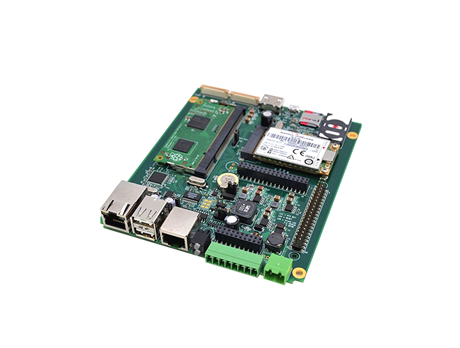
The Printed Circuit Board Assembly (PCBA) integration for Internet of Things (IoT) devices is a complex and crucial process that combines various electronic components onto a single printed circuit board (PCB) to enable seamless connectivity, data processing, and communication capabilities. IoT devices are designed to collect, transmit, and analyze data from the physical world, and the PCBA integration plays a vital role in ensuring their reliable and efficient operation.
The first step in PCBA integration for IoT devices is component selection. Given the diverse nature of IoT applications, components such as microcontrollers, sensors, wireless communication modules, and power management units need to be carefully chosen. For example, in a smart home IoT device, sensors like temperature, humidity, and motion sensors are essential for data collection. The microcontroller acts as the brain of the device, processing the sensor data and controlling other components. Wireless communication modules, such as Wi - Fi, Bluetooth, or ZigBee, are selected based on the required range, data transfer rate, and power consumption to enable seamless connectivity with other devices or the cloud.
Once the components are selected, the PCB layout design begins. This involves arranging the components on the PCB in an optimized manner to ensure proper electrical performance and signal integrity. In IoT devices, where multiple types of signals (analog, digital, and high - frequency) are present, careful consideration must be given to minimize interference between different components. For instance, high - frequency wireless modules should be isolated from sensitive analog components to prevent signal degradation. Additionally, power traces need to be designed with sufficient width to handle the current requirements of the components and reduce power losses.
After the layout design is complete, the PCB is fabricated using processes such as photolithography, etching, and plating. Then, the components are assembled onto the PCB through surface - mount technology (SMT) or through - hole technology. Quality control measures are implemented throughout the assembly process to ensure that all components are properly soldered and functioning correctly. Finally, the integrated PCBA undergoes comprehensive testing, including functional testing, electrical testing, and environmental testing. Functional testing verifies that the device performs its intended functions, while electrical testing checks for any short circuits, open circuits, or incorrect electrical parameters. Environmental testing, such as temperature and humidity testing, ensures that the PCBA can operate reliably in various real - world conditions.