-
CN
-
Service Hotline
+8618129931046 Mr. Liao


Time:2025-10-16 Views:1

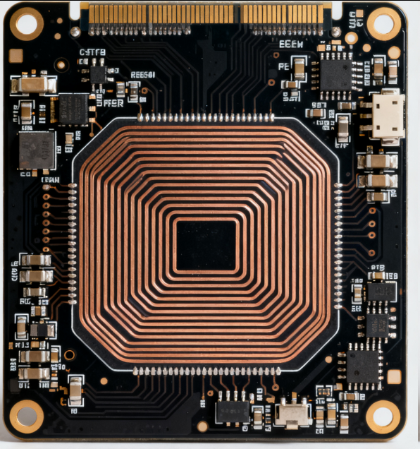
Printed Circuit Boards for wireless charging are essential components that enable the efficient transfer of electrical energy without the need for physical connectors. These PCBs play a crucial role in the design and functionality of wireless charging devices, from wireless charging pads to embedded wireless charging systems in smartphones, smartwatches, and other electronic gadgets. The design of PCBs for wireless charging is centered around optimizing power transfer efficiency, ensuring safety, and managing electromagnetic fields.
At the heart of wireless charging technology is the principle of electromagnetic induction or resonant coupling, and PCBs are designed to support these mechanisms. For electromagnetic induction - based wireless charging, PCBs house the coil - driving circuits. These circuits generate an alternating current (AC) that passes through the charging coil on the PCB, creating a changing magnetic field. The design of the coil - driving circuit on the PCB is critical, as it needs to precisely control the frequency, amplitude, and phase of the AC signal to maximize the power transfer to the receiving coil in the device being charged. High - performance power management integrated circuits (PMICs) are often integrated onto the PCB to regulate the input power, monitor the charging status, and protect against over - voltage, over - current, and short - circuit conditions.
In resonant - coupling - based wireless charging systems, the PCB design becomes even more complex. The PCB must support the creation of a resonant circuit, which requires careful selection and placement of components such as capacitors and inductors to achieve the desired resonant frequency. The layout of the PCB is optimized to minimize electromagnetic interference (EMI) generated by the high - frequency signals in the resonant circuit. Shielding techniques, such as using metal enclosures or conductive gaskets around the PCB, are employed to contain the electromagnetic fields and prevent interference with other electronic components in the vicinity.
Thermal management is another important aspect of PCBs for wireless charging. During the power transfer process, energy losses occur, which generate heat. PCBs are designed with large - area copper planes acting as heat sinks, thermal vias to transfer heat between layers, and sometimes even additional cooling components like heat pipes or fans in high - power wireless charging applications. Additionally, the materials used in the PCB construction are selected for their good thermal conductivity and high - temperature resistance to ensure reliable operation under continuous charging conditions. Overall, PCBs for wireless charging are engineered with a combination of advanced circuit design, component integration, and thermal management techniques to provide efficient, safe, and reliable wireless power transfer solutions.