-
CN
-
Service Hotline
+8618129931046 Mr. Liao


Time:2025-12-10 Views:1

SMT (Surface Mount Technology) PCBA assembly is a widely used electronic manufacturing process that mounts surface-mount components (SMDs) directly onto the surface of printed circuit boards (PCBs), replacing traditional through-hole technology for compact, high-density electronic products. This process is critical for manufacturing smartphones, laptops, IoT devices, and automotive electronics, where miniaturization and high production efficiency are essential.
The SMT assembly process consists of four core stages, each requiring precision equipment and strict quality control. First, solder paste printing uses a stainless-steel stencil with laser-cut apertures to apply a uniform layer of solder paste (a mixture of tin-lead or lead-free alloy particles and flux) onto the PCB’s solder pads. The stencil’s aperture size and thickness are tailored to component size—for example, 0402 chip resistors require 0.2mm×0.1mm apertures to ensure accurate paste deposition. Advanced printers (e.g., Fuji NXT III) integrate 3D solder paste inspection (SPI) to verify paste volume and shape, reducing defects caused by insufficient or excessive paste.
Second, component placement relies on high-speed pick-and-place machines equipped with vision systems. These machines (such as Yamaha YSM40R) can place up to 40,000 components per hour, including microchips (e.g., QFP, BGA, and 01005 ultra-miniature components). The vision system aligns components with PCB pads using fiducial marks, ensuring placement accuracy within ±0.02mm. For BGA components, special nozzles apply controlled pressure to prevent solder ball damage.
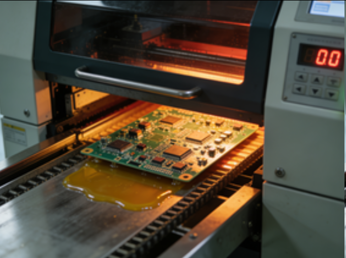
Third, reflow soldering heats the PCB in a temperature-controlled oven (typically 8–10 zones) to melt the solder paste. The oven’s temperature profile is optimized for the solder alloy—lead-free solder (e.g., Sn96.5Ag3.0Cu0.5) requires a peak temperature of 245–255°C, while leaded solder peaks at 215–225°C. This stage forms permanent electrical and mechanical bonds between components and the PCB.
Finally, inspection and testing use automated optical inspection (AOI) systems (e.g., Omron VT-S720) to detect defects like missing components, solder bridges, or tombstoning. For high-reliability applications (e.g., medical devices), X-ray inspection is used to check hidden solder joints (e.g., BGA underfill).
SMT assembly offers key advantages: it enables smaller PCB sizes (components occupy 60–70% less space than through-hole parts), higher production efficiency, and better electrical performance at high frequencies. However, it requires precise process control—even minor variations in solder paste viscosity or reflow temperature can cause defects.