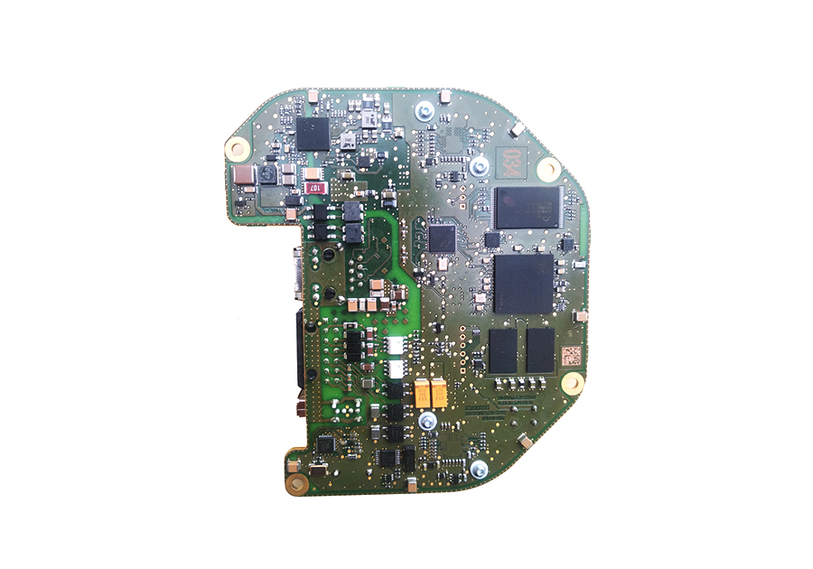
1. Miniaturization and High-Density Design
Consumer electronics devices are trending toward thinner, lighter, and more
portable designs, driving PCB designs toward smaller sizes and higher
integration densities.
Using HDI (High-Density Interconnect): This reduces board area through the
use of blind, buried, and microvias (aperture diameter ≤ 0.15mm). This is
commonly found in mobile phone motherboards and TWS earphone PCBs, with 4-12
layers.
Support for Mini LED/Micro LED backlighting: For display devices like
laptops and TVs, PCBs must integrate a large number of tiny LED driver circuits,
with line widths and spacings as small as 30-50μm.
Flexible PCBs (FPCs) are widely used in wearable devices (such as curved
watch screens) and foldable mobile phone screens. They are bendable, foldable,
and adaptable to unusual structures. 2. Prioritize Cost and Mass Production
Efficiency
The consumer electronics market is highly competitive, and PCB design must
balance performance and cost:
Substrate Selection: Mainly utilize conventional FR-4 substrate
(high-frequency substrate is only used in high-end devices such as flagship
phones) to reduce raw material costs;
Process Simplification: While ensuring performance, reduce unnecessary
advanced processes (e.g., avoid laser drilling in non-high-frequency
applications);
Compatibility with Mass Production: PCB design must comply with the
requirements of SMT automated production lines (e.g., standardized edge locating
holes and mark points) to avoid bottlenecks in mass production caused by
specialized processes. 3. Signal Integrity and High-Frequency Adaptation
As consumer electronics enter the "5G + WiFi 6" era, PCBs must ensure
stable high-frequency signal transmission:
Impedance Control: For 5G RF signals and high-speed data interfaces (such
as USB 3.2 and HDMI 2.1), PCB impedance must be precisely controlled (e.g., 50Ω
single-ended impedance, 100Ω differential impedance);
Anti-interference Design: Reduce signal crosstalk through ground isolation
(e.g., separate grounding for RF modules) and shielding layers (e.g., metal
shielding on mobile phone PCBs);
High-Speed Signal Optimization: Use equal-length traces and minimize the
number of vias to avoid signal delay or attenuation (e.g., DDR5 memory
interfaces in laptops). 4. Balancing Heat Dissipation and Reliability
As the power density of consumer electronics devices (such as fast-charging
mobile phones and gaming laptops) increases, PCBs must possess basic heat
dissipation capabilities:
Partially using aluminum or copper substrates: Heat generated in
heat-generating areas such as fast-charging modules and LED driver circuits is
quickly transferred through the metal substrate;
Increasing PCB copper area: Large copper areas are designed beneath the CPU
and power supply chips to enhance heat dissipation;
Compatible with consumer-grade reliability standards: Operating
temperatures and humidity ranges from -20°C to 70°C (some outdoor devices, such
as smart speakers, require -30°C to 85°C), and RoHS, REACH, and other
environmental certifications are required.


 Home >