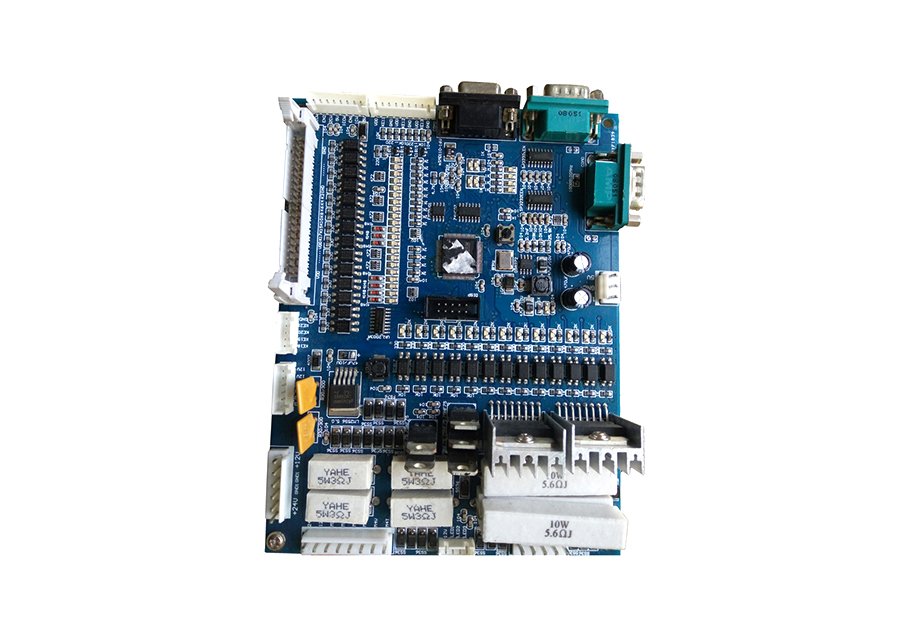
PCB PCBA Assembly Full Process Disassembly
1. Preliminary Preparation: Ensuring "Material and Process Matching"
Two key preparations must be completed before assembly to avoid process
adaptation issues:
Material Verification and Pretreatment
Bill of Materials (BOM) Verification: Confirm that component models,
packages (e.g., 0402 resistors, QFP chips), and parameters (e.g., capacitor
values, chip voltages) are consistent with the PCB design to avoid incorrect
materials.
Component Pretreatment: Bake damp components (e.g., ICs, BGAs) at 85°C for
12 hours to remove moisture and prevent "popcorning" (component cracking) during
soldering. Pretreat the pins of plug-in components (e.g., connectors) to remove
oxide layers.
Process File Development
Core Process File Output:
Stencil File (Gerber Format): Defines the solder paste printing area and
thickness (e.g., 0.12mm thick stencil for 0402 package, 0.15mm for QFP);
Reflow Oven Temperature Profile: Defines the heating zones (preheating
zone, constant temperature zone, reflow zone, and cooling zone) based on the
solder paste type (e.g., Sn63Pb37, lead-free SnAgCu). For example, the peak
temperature in the reflow zone for lead-free solder paste must be controlled at
240°C ± 5°C;
Placement Coordinate File: Defines the X/Y/Z coordinates and placement
angles of each component on the PCB to ensure accurate placement by the
placement machine.


 Home >